Classification of crystallographic defects (microscopic defects) is frequently made according to the geometry or dimensionality of the defect. Other macroscopic defects exist in all solid materials that are much larger than microscopic, these include pores, cracks, foreign inclusions, and other phases.
- Microscopic Defects
- Point Defects. Point defects have atomic dimensions.
- Line Defects. Line defects or dislocations are generally many atoms in length.
- Planar Defects. Planar defects are larger than line defects and occur over a two dimensional area.
- Macroscopic Defects
- Bulk Defects. Three-dimensional macroscopic or bulk defects, such as pores, cracks, or inclusions.
- Voids. Small regions, where there are no atoms, and which can be thought of as clusters of vacancies.
- Impurities, that can cluster together to form small regions of a different phase. These are often called precipitates.
Point Defects
Point defects have atomic dimensions, so that they occur only at or around a single lattice point. They are not extended in space in any dimension. Point imperfections in crystals can be divided into three main defect categories.
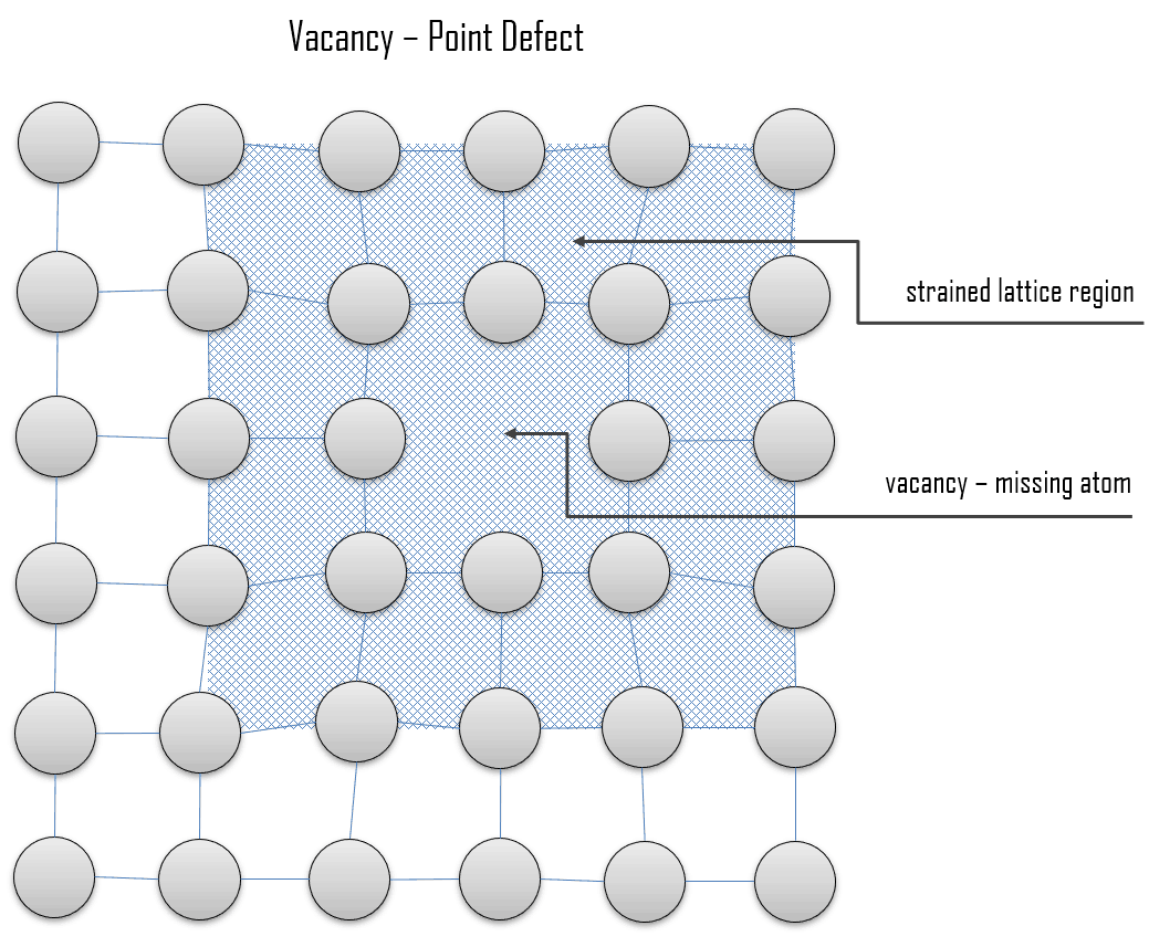
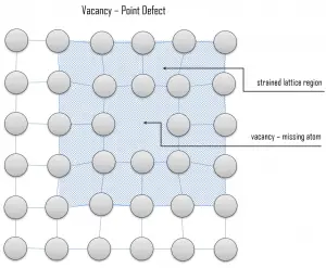 Vacancy defects. Vacancy defects result from a missing atom in a lattice position. The stability of the surrounding crystal structure guarantees that the neighboring atoms will not simply collapse around the vacancy. The vacancy type of defect can result from imperfect packing during the crystallization process, or it may be due to increased thermal vibrations of the atoms brought about by elevated temperature. All crystalline solids contain vacancies, and, in fact, it is not possible to create such a material that is free of these defects. A vacancy (or pair of vacancies in an ionic solid) is sometimes called a Schottky defect. This point defect forms when oppositely charged ions leave their lattice sites, creating vacancies. These vacancies are formed in stoichiometric units, to maintain an overall neutral charge in the ionic solid.
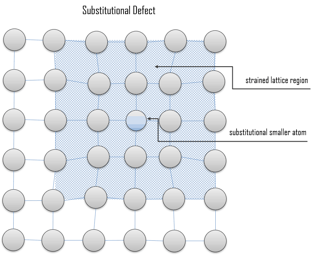
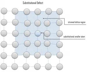 Substitutional defects. Due to fundamental limitations of material purification methods, materials are never 100% pure, which by definition induces defects in crystal structure. Substitutional defects result from an impurity present at a lattice position. For the substitutional type, solute or impurity atoms replace or substitute for the host atoms. Several features of the solute and solvent atoms determine the degree to which the former dissolves in the latter. These are expressed as the Hume–Rothery rules. According to these rules, substitutional solid solutions may form if the solute and solvent have:
- Similar atomic radii (15% or less difference)
- Same crystal structure
- Similar electronegativities
- Similar valency a solid solution mixes with others to form a new solution
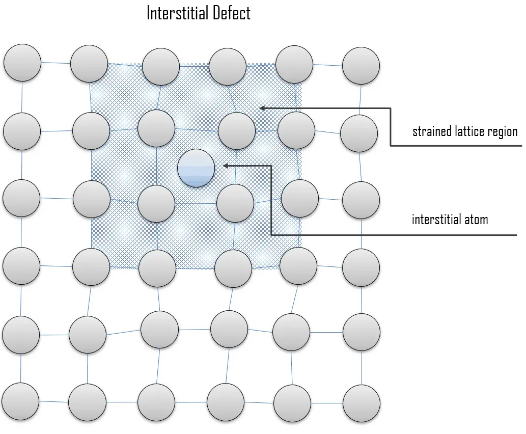
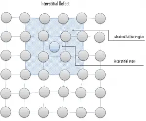 Interstitial defects. Interstitial defects result from an impurity located at an interstitial site or one of the lattice atoms being in an interstitial position instead of being at its lattice position. A self-interstitial is an atom from the crystal that is crowded into an interstitial site. In metals, a self-interstitial introduces relatively large distortions and stress in the surrounding lattice because the atom is substantially larger than the interstitial position in which it is situated. Interstitial defects are generally high energy configurations, on the other hand the formation of this defect is not highly probable. Small atoms (mostly impurities) in some crystals can occupy interstices without high energy, such as hydrogen.
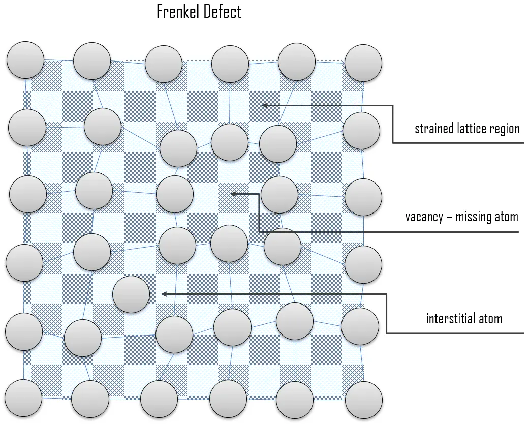
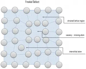 Frenkel Defects. A Frenkel defect or a Frenkel pair is a nearby pair of a vacancy and an interstitial defect. This is caused when an ion moves into an interstitial site and creates a vacancy. Their primary mechanism of generation is by particle irradiation. Frenkel defects are typical for radiation damage caused by high-energy neutrons. A 1 MeV neutron may affect approximately 5000 atoms. The presence of many displacement spikes will change the properties of the material being irradiated. A displacement spike contains large numbers of interstitials and lattice vacancies.
Line Defects – Dislocations
Line defects are generally many atoms in length. Line defects are called dislocations and occur in crystalline materials only. Dislocations are especially important in materials science, because they help determine the mechanical strength of materials. There are two basic types of dislocations, the edge dislocation and the screw dislocation. Mixed dislocations, combining aspects of both types, are also common. It is important to note that dislocations cannot end inside a crystal. They must end at a crystal edge or other dislocation, or they must close back on themselves.
Early materials studies led to the computation of the theoretical strengths of perfect crystals. But these theoretical strengths were many times greater than those actually measured. During the 1930s it was theorized that this discrepancy in mechanical strengths could be explained by a type of linear crystalline defect that has come to be known as a dislocation. The term ‘dislocation’ referring to a defect on the atomic scale was coined by G. I. Taylor in 1934.
Edge Dislocation
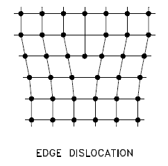
Edge dislocation centers around the edge dislocation line that is defined along the end of the extra half-plane of atoms. The imperfection may extend in a straight line all the way through the crystal or it may follow an irregular path. It may also be short, extending only a small distance into the crystal causing a slip of one atomic distance along the glide plane (direction the edge imperfection is moving). Macroscopic plastic deformation simply corresponds to permanent deformation that results from the movement of dislocations, or slip, in response to an applied shear stress. Dislocations can move if the atoms from one of the surrounding planes break their bonds and rebond with the atoms at the terminating edge. Understanding the movement of a dislocation is key to understanding why dislocations allow deformation to occur at much lower stress than in a perfect crystal. Dislocation motion is analogous to movement of a caterpillar. The caterpillar would have to exert a large force to move its entire body at once. Instead it moves the rear portion of its body forward a small amount and creates a hump. The hump then moves forward and eventual moves all of the body forward by a small amount. The slip occurs when the crystal is subjected to a stress, and the dislocation moves through the crystal until it reaches the edge or is arrested by another dislocation.
Screw Dislocation
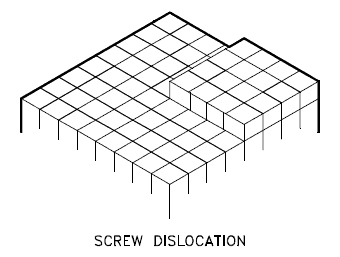
Screw dislocations can be produced by a tearing of the crystal parallel to the slip direction. If a screw dislocation is followed all the way around a complete circuit, it would show a slip pattern similar to that of a screw thread. A screw dislocation is much harder to visualize. Imagine cutting a crystal along a plane and slipping one half across the other by a lattice vector, the halves fitting back together without leaving a defect. The motion of a screw dislocation is also a result of shear stress, but the defect line movement is perpendicular to direction of the stress and the atom displacement, rather than parallel.
The pattern may be either left or right handed. This requires that some of the atomic bonds are re-formed continuously so that the crystal has almost the same form after yielding that it had before.
Source: William D. Callister, David G. Rethwisch. Materials Science and Engineering: An Introduction 9th Edition, Wiley; 9 edition (December 4, 2013), ISBN-13: 978-1118324578.
Planar Defects – Interfacial Defects
A planar defect is a discontinuity of the perfect crystal structure across a plane. Interfacial defects are boundaries that have two dimensions and normally separate regions of the materials that have different crystal structures and/or crystallographic orientations. Interfacial defects exist at an angle between any two faces of a crystal or crystal form. These imperfections are found at free surfaces, domain boundaries, grain boundaries, or interphase boundaries.
Grain Boundaries
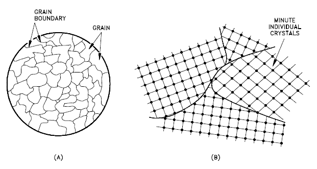
A grain boundary is a general planar defect that separates regions of different crystalline orientation (i.e. grains) within a polycrystalline solid. Up to this point, the discussion has focused on defects of single crystals. However, solids generally consist of a number of crystallites or grains of varying size and orientation. These have random crystallographic orientations. When a metal starts with crystallization, the phase change begins with small crystals that grow until they fuse, forming a polycrystalline structure. In the final block of solid material, each of the small crystals (called “grains“) is a true crystal with a periodic arrangement of atoms, but the whole polycrystal does not have a periodic arrangement of atoms, because the periodic pattern is broken at the grain boundaries. Grains and grain boundaries help determine the properties of a material. Grains can range in size from nanometers to millimeters across and their orientations are usually rotated with respect to neighboring grains. Where one grain stops and another begins is known as a grain boundary. Grain boundaries limit the lengths and motions of dislocations. Therefore, having smaller grains (more grain boundary surface area) strengthens a material. The size of the grains can be controlled by the cooling rate when the material cast or heat treated. Generally, rapid cooling produces smaller grains whereas slow cooling result in larger grains.
- Grains, also known as crystallites, are small or even microscopic crystals which form, for example, during the cooling of many materials (crystallization). A very important feature of a metal is the average size of the grain. The size of the grain determines the properties of the metal. For example, smaller grain size increases tensile strength and tends to increase ductility. A larger grain size is preferred for improved high-temperature creep properties. Creep is the permanent deformation that increases with time under constant load or stress. Creep becomes progressively easier with increasing temperature.
- Grain Boundaries. The grain boundary refers to the outside area of a grain that separates it from the other grains. The grain boundaries separate variously-oriented crystal regions (polycrystalline) in which the crystal structures are identical. Grain boundaries are 2D defects in the crystal structure, and tend to decrease the electrical and thermal conductivity of the material. Most grain boundaries are preferred sites for the onset of corrosion and for the precipitation of new phases from the solid. They are also important to many of the mechanisms of creep. On the other hand, grain boundaries disrupt the motion of dislocations through a material. Dislocation propagation is impeded because of the stress field of the grain boundary defect region and the lack of slip planes and slip directions and overall alignment across the boundaries. Therefore reducing crystallite size is a common way to improve mechanical strength, because the smaller grains create more obstacles per unit area of slip plane.
Twinning – Twin Boundaries
Twinning is a phenomenon somewhere between a crystallographic defect and a grain boundary. Like a grain boundary, a twin boundary has different crystal orientations on its two sides. But unlike a grain boundary, the orientations are not random, but related in a specific, mirror-image way. A twin boundary happens when the crystals on either side of a plane are mirror images of each other.
The boundary between the twinned crystals will be a single plane of atoms. There is no region of disorder and the boundary atoms can be viewed as belonging to the crystal structures of both twins.
There are three modes of formation of twinned crystals. Twins are either grown-in during crystallisation, or the result of mechanical or thermal work. Grown twins are the result of an interruption or change in the lattice during formation or growth due to a possible deformation from a larger substituting ion. Annealing or transformation twins are the result of a change in crystal system during cooling as one form becomes unstable and the crystal structure must re-organize or transform into another more stable form. Deformation or gliding twins are the result of stress on the crystal after the crystal has formed.
Bulk Defects – Volume Defects
Three-dimensional macroscopic defects are called bulk defects. They generally occur on a much larger scale than the microscopic defects. These macroscopic defects generally are introduced into a material during refinement from its raw state or during fabrication processes. These include cracks, pores, foreign inclusions, and other phases. The working and forging of metals can cause cracks that act as stress concentrators and weaken the material. Any welding or joining defects may also be classified as bulk defects.
- Three-dimensional macroscopic or bulk defects, such as pores, cracks, or inclusions.
- Voids — small regions where there are no atoms, and which can be thought of as clusters of vacancies.
- Impurities can cluster together to form small regions of a different phase. These are often called precipitates.
We hope, this article, Classification of Crystallographic Defects – Types, helps you. If so, give us a like in the sidebar. Main purpose of this website is to help the public to learn some interesting and important information about materials and their properties.