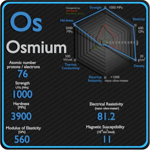
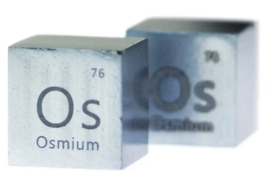
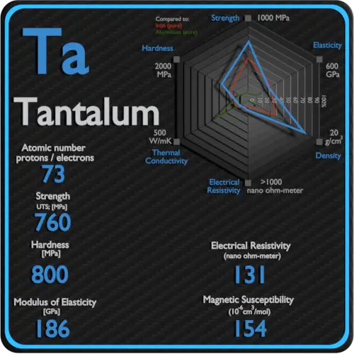
About Osmium
Osmium is a hard, brittle, bluish-white transition metal in the platinum group that is found as a trace element in alloys, mostly in platinum ores. Osmium is the densest naturally occurring element, with a density of 22.59 g/cm3. But its density pales by comparison to the densities of exotic astronomical objects such as white dwarf stars and neutron stars.
Electrical and Magnetic Properties of Osmium
Electrical property refers to the response of a material to an applied electric field. One of the principal characteristics of materials is their ability (or lack of ability) to conduct electrical current. Indeed, materials are classified by this property, that is, they are divided into conductors, semiconductors, and nonconductors.
See also: Electrical Properties
Magnetic property refers to the response of a material to an applied magnetic field. The macroscopic magnetic properties of a material are a consequence of interactions between an external magnetic field and the magnetic dipole moments of the constituent atoms. Different materials react to the application of magnetic field differently.
See also: Magnetic Properties
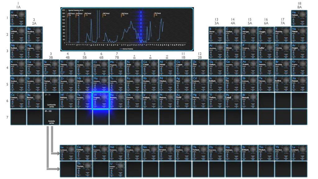
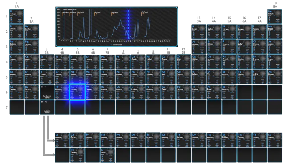
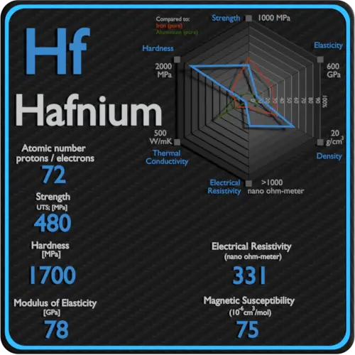
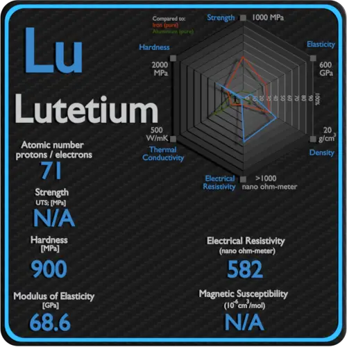
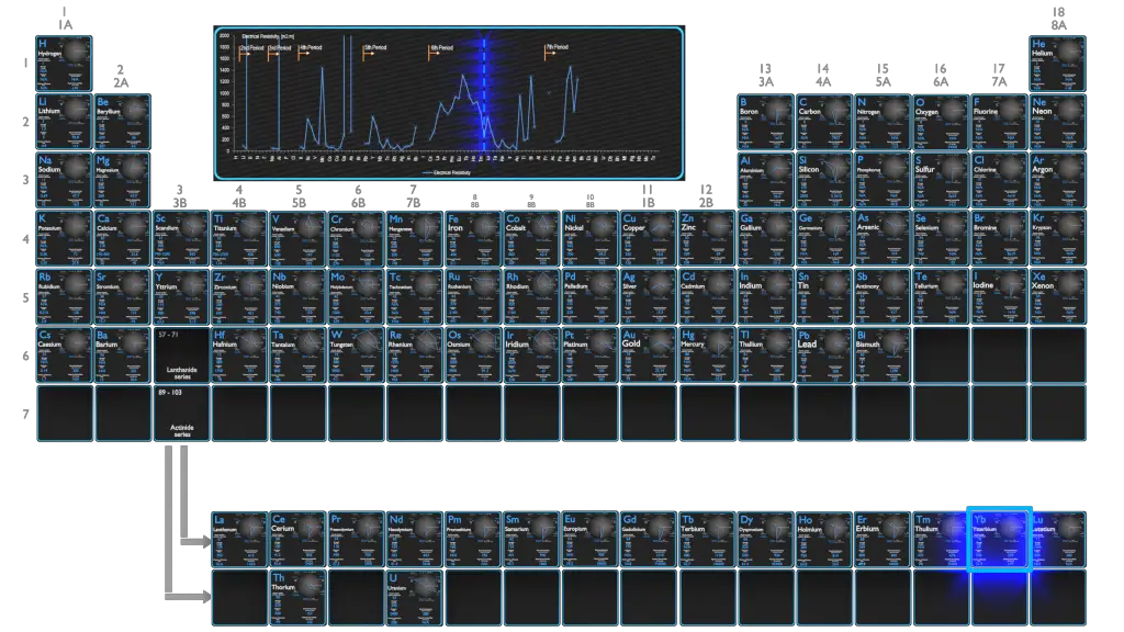
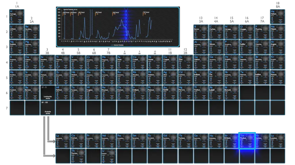
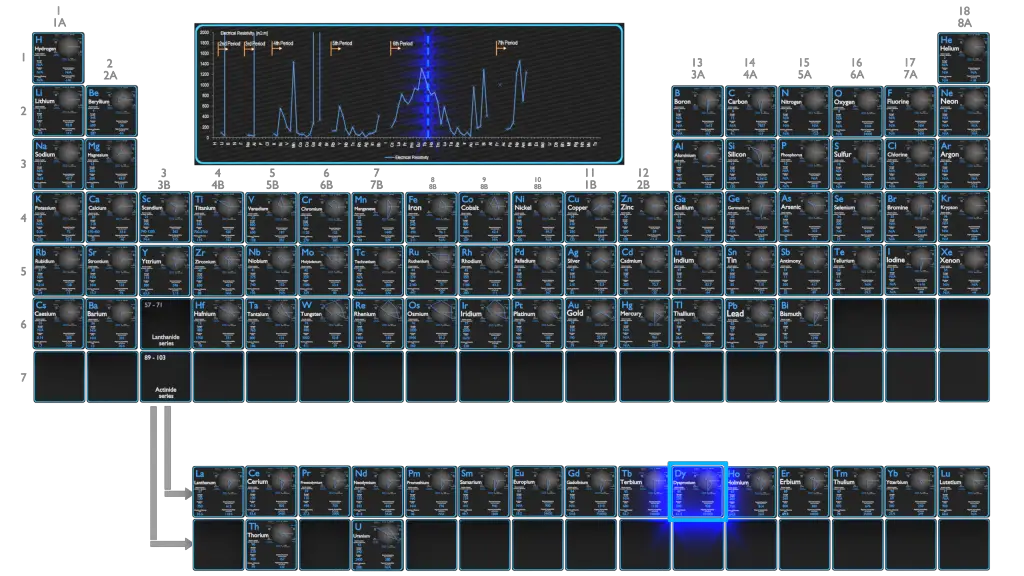
Electrical Resistivity of Osmium
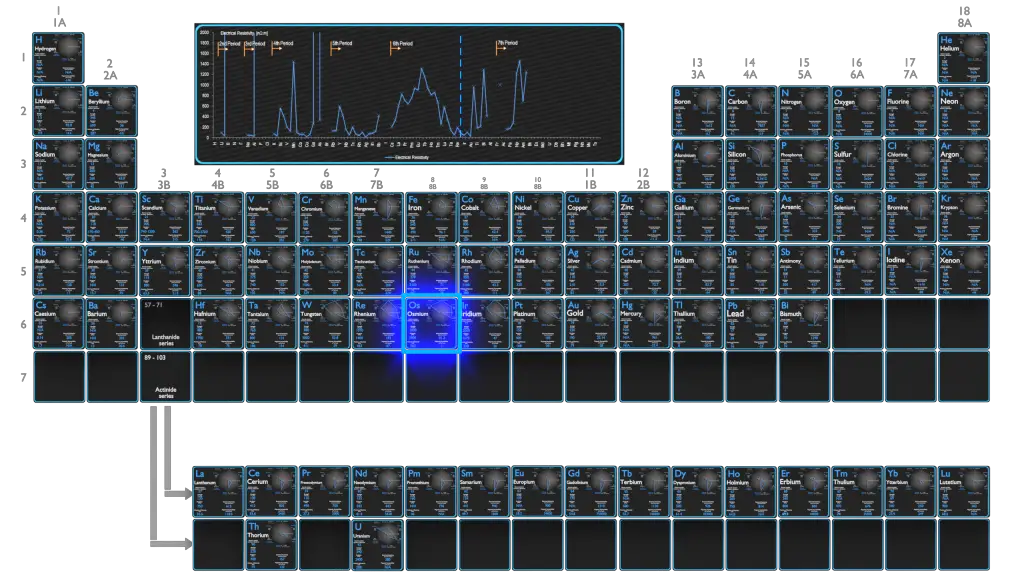
Electrical resistivity of Osmium is 81.2 nΩ⋅m.
Electrical conductivity and its converse, electrical resistivity, is a fundamental property of a material that quantifies how Osmium conducts the flow of electric current. Electrical conductivity or specific conductance is the reciprocal of electrical resistivity.
Magnetic Susceptibility of Osmium
Magnetic susceptibility of Osmium is +11e-6 cm^3/mol.
In electromagnetism, magnetic susceptibility is the measure of the magnetization of a substance. Magnetic susceptibility is a dimensionless proportionality factor that indicates the degree of magnetization of Osmium in response to an applied magnetic field.
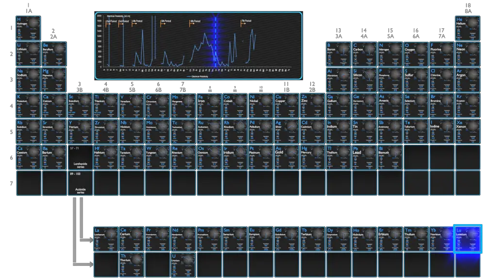
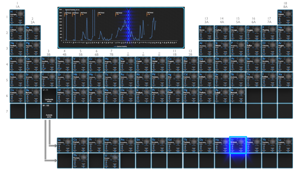
Electrical Resistivity of Elements
Magnetic Susceptibility of Elements
Electrical Resistivity of Chemical Elements
Electrical resistivity and its converse, electrical conductivity, is a fundamental property of a material that quantifies how strongly it resists or conducts the flow of electric current. A low resistivity indicates a material that readily allows the flow of electric current. The symbol of resistivity is usually the Greek letter ρ (rho). The SI unit of electrical resistivity is the ohm-metre (Ω⋅m). Note that, electrical resistivity is not the same as electrical resistance. Electrical resistance is expressed in Ohms. While resistivity is a material property, resistance is the property of an object.
Conductors – Semiconductors – Resistors
Substances in which electricity can flow are called conductors. Conductors are made of high-conductivity materials such as metals, in particular copper and aluminium.
Insulators, on the other hand, are made of a wide variety of materials depending on factors such as the desired resistance.
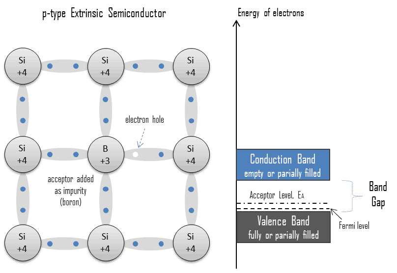
Semiconductors are materials, inorganic or organic, which have the ability to control their conduction depending on chemical structure, temperature, illumination, and presence of dopants. The name semiconductor comes from the fact that these materials have an electrical conductivity between that of a metal, like copper, gold, etc. and an insulator, such as glass. They have an energy gap less than 4eV (about 1eV). In solid-state physics, this energy gap or band gap is an energy range between valence band and conduction band where electron states are forbidden. In contrast to conductors, electrons in a semiconductor must obtain energy (e.g. from ionizing radiation) to cross the band gap and to reach the conduction band.
To understand the difference between metals, semiconductors and electrical insulators, we have to define the following terms from solid-state physics:
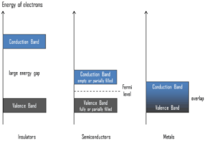 Valence Band. In solid-state physics, the valence band and conduction band are the bands closest to the Fermi level and thus determine the electrical conductivity of the solid. In electrical insulators and semiconductors, the valence band is the highest range of electron energies in which electrons are normally present at absolute zero temperature. For example, a silicon atom has fourteen electrons. In the ground state, they are arranged in the electron configuration [Ne]3s23p2. Of these, four are valence electrons, occupying the 3s orbital and two of the 3p orbitals. The distinction between the valence and conduction bands is meaningless in metals, because conduction occurs in one or more partially filled bands that take on the properties of both the valence and conduction bands.
- Conduction Band. In solid-state physics, the valence band and conduction band are the bands closest to the Fermi level and thus determine the electrical conductivity of the solid. In electrical insulators and semiconductors, the conduction band is the lowest range of vacant electronic states. On a graph of the electronic band structure of a material, the valence band is located below the Fermi level, while the conduction band is located above it. In semiconductors, electrons may reach the conduction band, when they are excited, for example, by ionizing radiation (i.e. they must obtain energy higher than Egap). For example, diamond is a wide-band gap semiconductor (Egap = 5.47 eV) with high potential as an electronic device material in many devices. On the other side, germanium has a small band gap energy (Egap = 0.67 eV), which requires to operate the detector at cryogenic temperatures. The distinction between the valence and conduction bands is meaningless in metals, because conduction occurs in one or more partially filled bands that take on the properties of both the valence and conduction bands.
- Band Gap. In solid-state physics, the energy gap or the band gap is an energy range between valence band and conduction band where electron states are forbidden. In contrast to conductors, electrons in a semiconductor must obtain energy (e.g. from ionizing radiation) to cross the band gap and to reach the conduction band. Band gaps are naturally different for different materials. For example, diamond is a wide-band gap semiconductor (Egap = 5.47 eV) with high potential as an electronic device material in many devices. On the other side, germanium has a small band gap energy (Egap = 0.67 eV), which requires to operate the detector at cryogenic temperatures.
- Fermi Level. The term “Fermi level” comes from Fermi-Dirac statistics, which describes a distribution of particles over energy states in systems consisting of fermions (electrons) that obey the Pauli exclusion principle. Since they cannot exist in identical energy states, Fermi level is the term used to describe the top of the collection of electron energy levels at absolute zero temperature. The Fermi level is the surface of Fermi sea at absolute zero where no electrons will have enough energy to rise above the surface. In metals, the Fermi level lies in the hypothetical conduction band giving rise to free conduction electrons. In semiconductors the position of the Fermi level is within the band gap, approximately in the middle of the band gap.
 Electron-hole Pair. In the semiconductor, free charge carriers are electrons and electron holes(electron-hole pairs). Electrons and holes are created by excitation of electron from valence band to the conduction band. An electron hole (often simply called a hole) is the lack of an electron at a position where one could exist in an atom or atomic lattice. It is one of the two types of charge carriers that are responsible for creating electric current in semiconducting materials. Since in a normal atom or crystal lattice the negative charge of the electrons is balanced by the positive charge of the atomic nuclei, the absence of an electron leaves a net positive charge at the hole’s location. Positively charged holes can move from atom to atom in semiconducting materials as electrons leave their positions. When an electron meets with a hole, they recombine and these free carriers effectively vanish. The recombination means an electron which has been excited from the valence band to the conduction band falls back to the empty state in the valence band, known as the holes.

Magnetic Susceptibility
In electromagnetism, magnetic susceptibility is the measure of the magnetization of a substance. Magnetic susceptibility is a dimensionless proportionality factor that indicates the degree of magnetization of a material in response to an applied magnetic field. The magnitude of M is proportional to the applied field as follows:

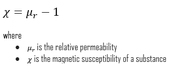
The magnetic susceptibility and the relative permeability are related as follows:
 This allows a simple classification of most material’s response to an applied magnetic field into two categories: an alignment with the magnetic field, χ>0, called paramagnetism, or an alignment against the field, χ<0, called diamagnetism.
- Diamagnetic Material. Diamagnetic materials are those that some people generally think of as non-magnetic. Diamagnetic materials are repelled by a magnetic field; an applied magnetic field creates an induced magnetic field in them in the opposite direction, causing a repulsive force. Diamagnetism results from changes in electron orbital motion that are induced by an external field. Diamagnetic materials include water, wood, most organic compounds such as petroleum and some plastics, and many metals including copper, particularly the heavy ones with many core electrons, such as mercury, gold and bismuth. The effect is extremely small (with susceptibilities on the order of -10-5) and in opposition to the applied field. Diamagnetic materials, like water, or water-based materials, have a relative magnetic permeability that is less than or equal to 1, and therefore a magnetic susceptibility less than or equal to 0, since susceptibility is defined as χv = μv − 1. Diamagnetic and paramagnetic materials are considered nonmagnetic because the magnetizations are relatively small and persist only while an applied field is present. If χ (magnetic susceptibility) is negative, the material is diamagnetic. In this case, the magnetic field in the material is weakened by the induced magnetization. Diamagnetic materials are repelled by magnetic fields. For example, the magnetic susceptibility of diamagnets such as water is χv = −9.05×10⁻⁶. The most strongly diamagnetic material is bismuth, χv = −1.66×10⁻⁴. Generally, nonmagnetic materials are said to be para- or diamagnetic because they do not possess permanent magnetization without external magnetic field.
- Paramagnetic Materials. Paramagnetic materials are those having permanent atomic dipoles, which are acted on individually and aligned in the direction of an external field. Diamagnetic and paramagnetic materials are considered nonmagnetic because the magnetizations are relatively small and persist only while an applied field is present. If χ (magnetic susceptibility) is positive, a material can be paramagnetic. In this case, the magnetic field in the material is strengthened by the induced magnetization. Paramagnetic materials include most chemical elements and some compounds. They have a relative magnetic permeability slightly greater than 1 (i.e., a small positive magnetic susceptibility) and hence are attracted to magnetic fields. Generally, nonmagnetic materials are said to be para- or diamagnetic because they do not possess permanent magnetization without external magnetic field.
A closely related property of materials is the relative permeability, which is the ratio of the permeability in a material to the permeability in a vacuum. In general, the permeability is the measure of the resistance of a substance against the formation of a magnetic field.
Neither μr nor χ are constants, , as they can vary with the position in the medium. They depend not only on the material but also on the magnitude of the field, H, the frequency of the applied magnetic field, humidity, temperature, and other parameters. Nearly all materials respond to a magnetic field by becoming magnetized, but most are paramagnetic with a response so faint that it is of no practical use. A few, however, contain atoms that have large dipole moments and have the ability to spontaneously magnetize (i.e. to align their dipoles in parallel). These are called ferromagnetic and ferrimagnetic materials (the second one is called ferrites for short), and it is these that are of real practical use. Ferromagnetic, ferrimagnetic, or antiferromagnetic materials possess permanent magnetization even without external magnetic field and do not have a well defined zero-field susceptibility.
Summary
| Element | Osmium |
| Atomic number | 76 |
| Element category | Transition Metal |
| Phase at STP | Solid |
| Electrical resistivity [nanoOhm meter] | 81.2 |
| Magnetic Susceptibility | +11e-6 cm^3/mol |
Source: www.luciteria.com
Other properties of Osmium


